-
ELPIS’s
proprietary technology LPS(Laser Pattern Structuring), which enables diverse plating on all engineering plastics to increase mechanical and electronical performance, is being widely adopted across IT and automobile sectors.
-
LPS technology
was developed by ELPIS’s CEO, Mr. Kwon in 2013 and applied for LMA(Laser Mould Antenna) of smartphones on large scale production.
-
MID
(Moulded
Interconnection
Device) together with LPS technologyTraditional MID ) requires special resin containing additive to fasten copper layer onto 3D injection mould. What sets ELPIS’s MID apart from others is that you do not need such special resin. LPS(Laser Pattern Structuring) enables direct circuit on 3D injection mould made out of any engineering plastics. With ELPIS’s MIDs, you can bring mechanical and electrical engineering together into a complete product, combining the circuitry, housing, connectors, and cables into one whole part. In the world of MIDs, there isn’t a separate circuit board or an enclosure anymore, which reduces BOM complexity, improves reliability, and reduces costs.

applying LPS was first debuted on a plating journal in 2013

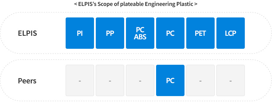
Since 2013 when ELPIS first introduced LPS technology to the market, multiple peers also provide LPS solution, however, ELPIS is still the only one who can apply LPS technology to divers engineering plastics as follows.

-
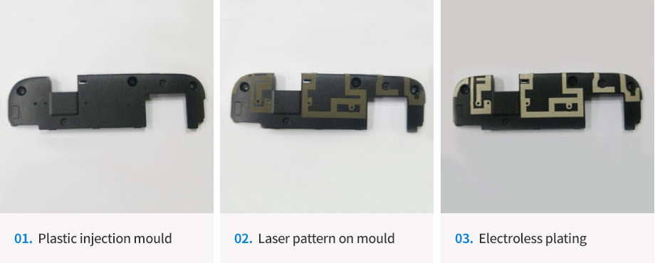
Case study of LMA(Laser Mold Antenna) - LPS
- -
As a plating solution provider, ELPIS has a track record of mass production of LMA with over 98% of yield ratio.

- -
-
Case study of automotive electronic parts - LPS
- -
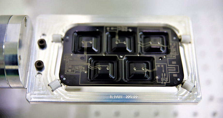
ELPIS is developing a button-type gear panel as a automotive electronic part which requires high degree of reliability.

- -
-
Case study of MID - LPS
- -
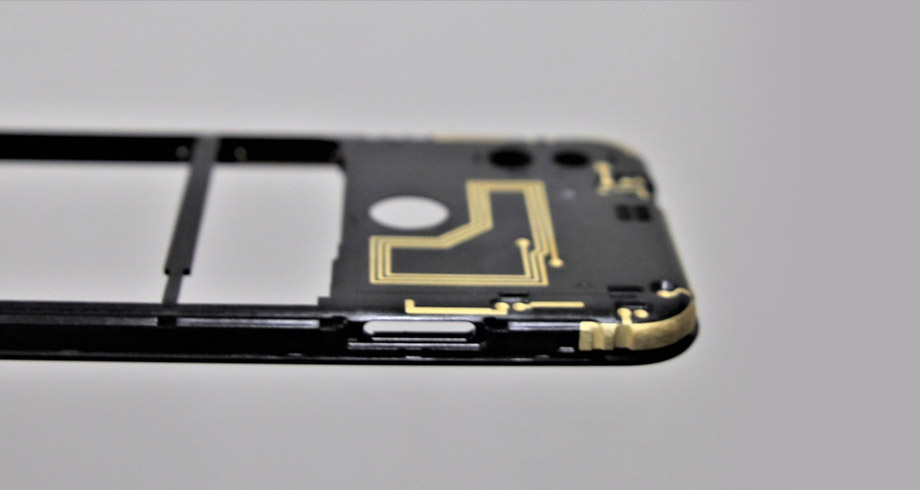
ELPIS is developing a MID for smart phone middle cases onto which you can directly mount antennas and chips.

- -


